


Click more than once to enlarge
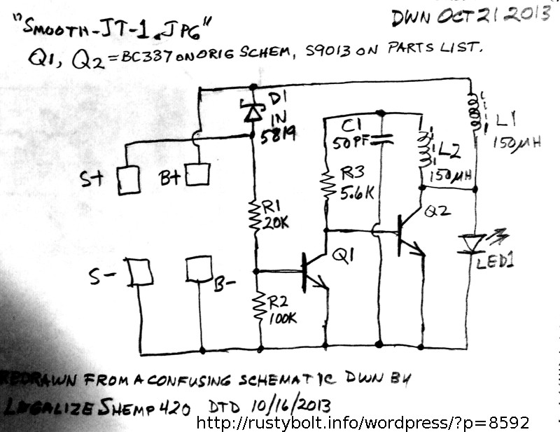
I came across a schematic of a “Joule Thief” circuit, actually a two transistor LED V boost circuit, on OverUnity.com. This is part of a garden light, and has a solar cell to recharge the battery, and the battery to store the electricity until after dark. The schematic, dated 10/16/2013, was drawn partially upside down and it was confusing to understand how it worked. I redrew it according to more conventional ways of drawing a schematic, such as input on the left, power at the top, common or ground at the bottom and output on the right. I checked and double checked my drawing to make sure it was the same as the original.
The first problem I saw was that the Q1 base bias did not look like it would work. The R2 100k resistor is connected from the Q1 base to common negative, which is okay. But the R1 20k resistor is connected to the positive of the solar cell. This might have a positive voltage when the sun is shining, but that is when the light should be off. Then after dark, there is no voltage across the solar cell, and no positive voltage across R1 to supply base bias current to Q1. So I don’t see how the light would work at night.
The D1 1N5819 Schottky diode is connected from positive of the solar cell to positive of the battery, but it conducts only when the sun is shining. After dark, the D1 is reverse biased and conducts no current to the R1. It should be effectively an open circuit.
I checked the data sheet for the S9013, and found that it’s capable of handling a half amp, which is about the same as the 2N4401 or PN2222A, and also has the same pinout. There are several gain ranges, and if I had a choice, I would pick one of the higher ones when purchasing them.
The circuit is similar to other two transistor circuit designs, however almost all two transistor designs use a single choke, but this circuit uses two chokes. This is one of the more expensive components in the circuit, so eliminating the second one would save money, unless there is something important that it does in the circuit that would justify keeping it in the circuit. Apparently other circuit designers didn’t think it was necessary or important.
I’ve thought about the possibility that Q1 does nothing while it’s operating, and is only there to turn it off during the daytime. If that is the case, the only way that it can work is if the two chokes are acting as one coil with the external magnetic field coupling them together. The two chokes are close together, but they are positioned end to end, not side by side. The coupling while end to end is not as good as if they were side by side. I have built one of these before but I consider them to be a poor design, because the circuit may work poorly or not at all if the two chokes are positioned wrong, are polarized wrong or have been wound differently.
I’m intrigued by what might be happening with this circuit, especially with the function of L2 and C1. I’m seriously considering putting the circuit together next weekend, but I’m pretty sure that it will not work with the bias problem. I thought that the author may have made a mistake when he drew the schematic. I have considered trying to contact the author on OU, but decided against it. I only log onto this OU forum once every few months, and in the past it has deleted my account because I didn’t log on often enough. Or else it required a “secure” password and complained when I tried to use one of mine, so I had to choose another and I don’t have a snowball’s chance in hell of remembering it after a few months. And I’m sick and tired of having to jump through so many hoops to recover my password that I’ve decided not to waste time doing it again and again. So that’s why I’m posting it here.
Update Oct 27 – Hanspeter left a comment and gave a link to the circuit (in German) (I ran it through Google translate). Thank you, Hanspeter, for showing us another almost identical circuit that uses the same principles. The author confirms my assessment that the Q1 is only used to shut off the LED during the daytime. This must mean that the feedback to keep it oscillating is from magnetic field coupled to the choke L2. I’m not sure what the C1 does. Again, the author’s schematic shows the base bias for Q2 is also taken from Q2’s collector, which doesn’t make much difference because the DC resistance of L1 is low, only a few ohms.
One thing that this circuit manages to do is save money by not using a two winding coil. The chokes are less expensive in large quantities, and act as a coil when positioned close to each other. But if the circuit was designed to use the second transistor to both invert the feedback signal and shut it off in the daytime, then the second choke could be eliminated. I assume that a transistor is cheaper than the choke, so even if a third transistor is added, the circuit would still be cheaper than with two chokes.


Hallo,
Hier ein Link zu dieser Schaltung.
http://www.b-kainka.de/bastel124.htm
Gruß hape
Danke.