


First off, I must state that the PSO is not the best solution for an audio oscillator. It uses only a single transistor, but it has a limitation that makes it put out a poor quality sine wave. As typical of the PSO, the sine wave becomes distorted because the loop gain is greater than unity and the amplitude of the sine wave grows until the transistor goes into either saturation or cutoff, and the sine wave gets clipped. If you want a clean, stable sine wave, then use a Wien Bridge Oscillator.
 The previous JFET PSO was so finicky about adjustment that I was very concerned that it would not work if the temperature changed. I found a PSO schematic that said that the gain of the amplifier decreases when a suitable level is reached. But how? I thought. One way to find out if this was the case was to build the circuit. I tack soldered the parts together and it oscillated when powered up. I checked the scope and found that the sine wave was not quite what I had expected but it was better than many other PSO sine waves.
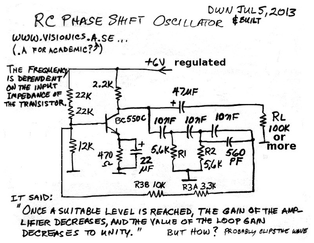
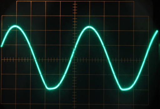
So I proceeded to make some changes to the circuit to get the sine wave to look better (see the o’scope photo). I used a pot to vary the value of the two 22k resistors that set the base bias. The changes are shown in the schematic. I chose a very high gain transistor because its higher input impedance is less of a load on the CR network, but a 2N3904 or similar should work. It just happened to be that the frequency was just a bit over 1 kHz, 1024 Hz or so. I added the 560 pF capacitor to lower the frequency down to about 1008 Hz, but since the three 10 nF capacitors are 5 percent tolerance, the difference between sets may be enough to need more or less added capacitance. It would probably be better to use a 5.1k for one of the resistors, and put a 1k pot in series so the frequency can be adjusted higher or lower.
It showed the RL as 100k or more. The reason is that the load changes the gain of the transistor and can change the amplitude of the sine wave or even stop it from oscillating. The best solution to this would be to add another transistor to buffer the sine wave and prevent load changes from changing the oscillation. The original circuit had only R3A, the 3.3k resistor. I added the 10k R3B to reduce the feedback somewhat so it wouldn’t cause so much distortion in the sine wave. It also lowered the frequency slightly; the reason is the transistor’s base, the two base bias resistors and R3 A and B are the actual resistive part of the third CR section. This should be closer to the 5.6k of the two other resistors, but it isn’t, it’s more than R3 A and B, which is 13.3k.
I found the formula for calculating the frequency at several websites. They say it’s 1 / 2 / Pi / square root of 6 / R / C or .065 divided by R, divided by C. In both cases, R and C must be in their fundamental units, such as 5600 for R, which is 5.6k, or .00000001 for C which is 0.01 microfarad. If your calculator has exponent, then you can use E-6 for microfarads or E-12 for picofarads.
I have calculated the values for the schematic shown, and it is assumed that the third CR section, which is actually the resistance of R3A, R3B, and the input of the transistor, But the input depends on the gain of the transistor, so it may change with different transistors. The 12k and two 22k resistors are about equal to 9.4k, plus the R3 A and B, for a total of about 22k. That is much more than 5.6k, so the formula gives a different answer than the 1008 Hz that’s the actual frequency – it’s more than ten percent higher. The conclusion that I make is that for a regular transistor, the formula is not accurate enough due to the unknown resistance of the transistor and its bias resistors. It should be okay for a JFET which has a very high input impedance. But that’s not the case for a single BJT. I could use two transistors in a compound connection similar to a Darlingoton, which would raise the input impedance a hundred times or more. Then the base bias resistors would be almost all of the input impedance.
Measurements
The supply voltage was 6.0V. I measured the voltage across the 470 ohm emitter resistor at 0.65V. That would be about 1.38 mA. I measured the total supply current at 1.5 mA, so that seems about right given the base bias resistors take some small amount of current. The actual frequency was 1008 Hz; according to the formula it should be 1160 Hz. The scope shows a slight clipping at the bottom of the sine wave. I adjusted the supply voltage and found a point where the distortion was minimal, but this point was at an odd voltage. To get that point to 6V, the bias resistors would have to be changed. It would oscillate at 5V or 9V if the bias was changed.
Update Jul 11 – I removed the 10k in series with the 3.3k, so that the value of R in that last CR section is more equal to the other 5.6k resistors. The frequency moved up to 1091 Hz. The 12k and 44k resistors in parallel are equal to 9.43k. In addition the 3.3k resistor in series makes 12.73 k. When the transistor’s resistance is included, I’d guesstimate the combined resistors is somewhere close to 10k. That’s almost twice the 5.6k resistors.
The sine wave had a bit more distortion in it. I decided that I could add resistance to the 22 uF emitter bypass capacitor to reduce the gain of the transistor and lower the distortion. I unsoldered one end of the 22 uF and put a 100 ohm trimpot as a variable resistance in series with the lead. I set the trimpot at minimum and powered up the circuit. The sine wave looked like it did before, so I turned the trimpot up. The sine wave got less distorted but then the oscillations died. The trimpot setting was very touchy; just a small change from the low distortion setting to no oscillation. I adjusted it as best as I could for low distortion, shut it down and measured the trimpot resistance, and it was 36 ohms.
Which brings me back to the point where I was when I did the JFET PSO. With the gain lowered to get the minimal distortion, the gain is at the point where it equals the loss of 29 in the CR network. This wouldn’t be a problem, except as the temperature changes, the transistor’s gain changes, dropping as the temperature gets colder. If this circuit was exposed to cold temperatures, I’m sure that it would stop oscillating. What is needed is a feedback loop that adjusts the gain, depending on how high the output voltage is. As the gain changes, the feedback loop compensates for it and holds the output voltage at a point below where it starts to distort. I’m writing a blog about changing a trimpot in a circuit so that it is not as sensitive.
BOGUS Circuits
I found this web page with a photo with two PSO circuits, one a transistor and the other with an opamp. The transistor does not have an emitter resistor with a bypass capacitor. This means if the supply voltage changes just slightly, the operating point will change and cause the sine wave to become distorted or stop altogether. The circuit has four CR sections, but the resistors are 1k, which is much lower than the 3.3k collector resistor, and that loads it down too much. The values of this circuit were poorly chosen.
The opamp circuit is bogus, and will not work. The two 1k resistors of the CR sections should be connected to ground. They are shown connected to the feedback line. That’s a major mistake. If the website admins knew something about electronics, they would have caught this, but they don’t, apparently. Instead, some unsuspecting experimenter will try to build the circuit and become frustrated when they cannot get it to work. Long ago I complained to someone about a major mistake. The reply I got was “You got what you paid for.” They were implying that they paid nothing, so they should not expect to get something for nothing. I think that was a very bad attitude. It also showed that many of these websites are not concerned about the interests of the viewer, all they are concerned about is getting people to view their advertising. I think that is also a bad attitude. And think about this: the website is making money from the hits or views they get from viewers, so the viewer in turn should reasonably expect to get something for their view.
Back to experimenting…


Phase Shift Oscillator
The Phase Shift Oscillator uses the charging of a capacitor via a resistor to produce a time delay. In this circuit, there are three time-delay sections made up of a 22n and 10k resistor, with the third delay using the base-emitter junction as the resistor. The operation of the circuit is very complex, so we will simplify the description.
The output is a smooth rising-and-falling waveform – a SINEWAVE.
When the power is applied to the circuit the transistor will immediately turn on FULLY as the three 22n capacitors will acts as “short-circuits” and current will pass to the base and the collector voltage will fall to a very LOW level.
The capacitors will gradually charge via the 10k resistors and the voltage across the second 10k resistor will drop (due to the charging current into the middle 22n gradually reducing) and the voltage on the left lead of the 3rd 22n will drop. This will reduce the voltage on the right lead of the 22n and turn the transistor OFF. The first two 22n’s will start to charge but the voltage across the 2nd 10k will be very small and the 3rd 22n will start to charge via the 1M resistor.
The charging of the first 22n is much faster than the charging of the third 22n and the voltage on the output rises to almost rail voltage. This allows the 3rd 22n to charge at a faster rate and just when the collector voltage reaches a maximum, the base voltage reaches 0.6v and the transistor starts to turn ON.
This lowers the collector voltage but the transistor still keeps turning ON via the 1M and the three 22n start to charge. This action increases the “turn-ON” of the transistor and it continues to turn-ON until the voltage on the collector reaches a very LOW level.
The circuit works completely differently to anything described in any Text Book. The transistor operates on a rising and falling CURRENT (increasing and decreasing current) into the base. That’s why no-one has described it before.
The third 22n continues to charge and the “turn-ON” current for the transistor reduces and it starts to turn OFF a slight amount. The second 10k continues to charge the middle 22n and the voltage across the 10k reduces. This pulls the left lead of the third 22n towards the 0v rail and the right lead follows. This action turns OFF the transistor and the collector voltage rises.
Most descriptions I’ve read of the PSO explain the actions in the frequency domain, which you do not do, instead you attempt to explain it in the time domain: capacitors charging discharging, turning ON and Off, etc. Others explain it in the frequency domain, since it is happening at a fixed frequency: 60 degrees phase shift per CR section, 180 degrees shift total, etc., which you do not talk about at all. The transistor’s base does become part of the resistance of the third CR section, but it is non-linear, since it is essentially a diode junction. Since it is still a (dynamic) resistance, the rising and falling current you talk about still develops a rising and falling voltage across the B-E junction, no matter how non-linear it may be. Therefore I disagree with your “competely different” statement.
I enjoy looking at your comprehensive web pages, but I find many incongruities that are, IMHO, at odds with what is out there in textbooks and educational institutions ( I work for one, BTW). The above is just another example. Thank you for your comments.