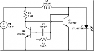
 Quantsuff gave me permission to post his schematic of the two NPN transistor voltage booster, often mislabeled a Joule Thief. This uses an NPN transistor to drive the output transistor, which is also NPN. The commonest two transistor V booster uses a PNP to drive the NPN output transistor, and for good reason, as I explain below.
I should explain why I know a bit about this circuit. I first started using the single transistor voltage booster, later known as the Joule Thief, more than ten years ago but due to my inexperience with the very high current demand on the transistor, I didn’t get the performance that I was expecting. So I changed to the two transistor designs, including this one. I got better performance from these so I used the two transistor design to build my first batch of single cell LED lights.
Demanding – There are at least two criteria that must be met to get this circuit to put out enough current to the LED. First off the output transistor Q1 must be able to switch high enough current. When this transistor is fully on, the collector voltage should be less than 1/4 volt. Then the resistor R1 supplies the current to cause Q1 to saturate, so this resistor must be low enough to allow that high current. Remember that the supply voltage is only 1.5V, and the base to emitter voltage is at least 0.6V (probably more like 0.7 or maybe more), so the voltage across R1 is less than 0.9V. I used a BC337 for Q1 and I used a 470 ohm resistor to get the Q1 base bias current up high enough to cause Q1 to fully saturate. But my calculations show that it might be 100 ohms or even less.
Once we get Q1 to saturate, we then need to get it turned off. In order to do this, Q2 must shunt the base current of Q1 to ground. Q1 must turn fully on and drop its collector voltage to less than 0.6V, which is the base voltage of Q1. So R2 has to be low enough to cause Q2 to fully turn on and saturate. Thus, R2 must be less than a certain value depending on the current gain of Q2. I put a 100k pot there and adjusted it lower and higher. At the higher settings the collector voltage of Q2 / base voltage of Q1 was too high and the circuit put out less light and drew excessive current.
Some experimenters love to put adjustable resistors AKA pots in there and see what the circuit does. A good designer will calculate the resistance value assuming minimum supply voltage and minimum gain for the transistors, and then use that value in the circuit. But there’s not much fun then, is there? One other point. The circuit must have enough gain to start oscillating when powered up. The gain of Q2 must be high enough to get it oscillating.
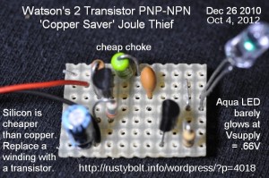
 The PNP – NPN version of this circuit (see photo) is different in that when Q2 turns on, its collector current turns on Q1’s base, and therefore the Q1 base current is not determined by the resistance. Instead it is determined by how hard Q2 is turned on, and that could be tens of milliamps.
Back to experimenting…


Where can i find the shematics of the second
PNP – NPN version ?
Did you try the link I gave at the beginning of the blog to Quantsuff’s website? He has at least one version.
Ahh ok, thanks. I did not find that link cause its the first word of the blog:-(
I will check all your blog-emtrys…in the next days, you got nice stuff here!
I came to youre site from yotube.
Thanks for now and thanks in the name of all for your work here.
Daniel
A.If I add a 5V zener Diode from the base of Q1(Anode) to The output(Through a schottky diode and an inductor), Would it regulate to 5V?
B. Can I remove the capacitor? (The speed up capcitor on Q1’s Base?)
Thanks. Miracletech.
A. Use this schematic with the zener voltage that you need.
https://www.seventransistorlabs.com/tmoranwms/Circuits_2010/Blocking_Oscillator_Supply.png
For more information on this schematic see my 2013-06-05 blog
https://rustybolt.info/wordpress/?p=6515
B. You can remove the capacitor but the performance may not be as good. Try different values to see what happens.
Sorry for my late replies, But I just came across this one:
https://www.google.com/imgres?imgurl=https://patentimages.storage.googleapis.com/25/36/a5/d3d6c21187abd5/US06597155-20030722-D00000.png&imgrefurl=https://patents.google.com/patent/US6597155B2/en&h=120&w=269&tbnid=778ruZffKwB52M&q=self+oscillating+boost+converter&tbnh=50&tbnw=113&usg=AI4_-kQhAhRwtzB6wNEfEMTgdHo4Crt-Yg&vet=1&docid=MoEmGfESQGSk7M&client=ms-opera-mini&sa=X&ved=2ahUKEwjetPTfkM7sAhWFCOwKHTY2Dm4Q9QEwAHoECAAQBA
Sorry for long link, But won’t it work?
Also, You didn’t explain how the circuit works in total, Could you explain it?
Thanks, Miracletech.
The energy is stored in the magnetic field of the coil when the transistor is on. Then when the transistor is off, the energy is released at a higher voltage into the load, which is the LED.
I understand how a Boost converter works, But I’m confused how it oscillates. I don’t get how Q1 turns on, And then Q2 Turns off and vice versa. How does the transistors switch between states?
You have to remember that there is no positive feedback when the magnetic field is not changing. When the magnetic field turns on, ramps up and reaches the point where it’s at its maximum, the feedback no longer keeps the base turned on. So that’s when the magnetic field starts to collapse. As it does the feedback now turns the transistor off. When it’s off, the cycle repeats. This is similar to the astable multivibrator.
Thanks. I get it now. I appreciate your dedication to answer.
For anyone else reading this, This circuit Works.
You’re welcome.