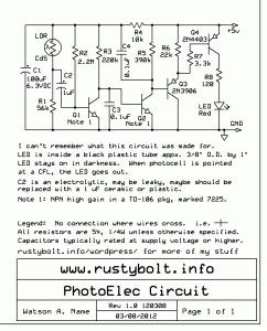
 I built this circuit long ago and I can’t remember what I intended it to be used for. It’s kind of different. The CdS photocell is glued into the end of a 3/8 inch O.D. by 1 inch long piece of black plastic, probably cut from the body of a cheap ball point pen. This makes the photocell directionally sensitive.
CdS photocells are slow to begin with. Also, the 56k R1 is a high resistance so the light level must be relatively low. The CdS photocell is AC coupled to the rest of the circuit so the circuit was meant to respond to changes in light level. The circuit uses four transistors which means it has a very high gain and hence high sensitivity (more about this below). The R4 and C1 bypass the power supply to ground or common. The coupling capacitor C2 is large for good low frequency response and the low pass capacitors C3 and C4 limit the bandwidth to very low frequencies, so I believe that it was not for a remote, but for some form of motion sensing. As I block and unblock the light on the photocell, I can tell from the LED’s slowness that the circuit performs only for slow changes in light.
The Q1 and Q2 transistors are very high current gain, more than 500. I got them from some surplus place and they are numbered 7225, an odd number, probably a part number for some company’s inventory. They are in the TO-106 package, which is no longer being made. Both the TO-105 and the larger TO-106 packages were very popular. It’s a drop of black epoxy on top of a ceramic cup. I remember reading someone’s recollections about this at one time popular transistor package. The company (Fairchild or National?) received an order for thousands of the transistors. They asked the customer what kind of transistor they would like. The customer replied that they didn’t care; they were going to use them for the eyes on their teddy bears. (!)
I’ll have more to say when I do some more experimenting with it.