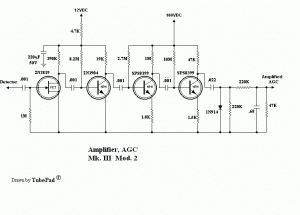
 Leonard Meeks posted a schematic of Mk.7 Mod 2 AGC amplifier to the Regenrx Yahoo group. I’ll include it here.
The amp uses a FET for the input stage, a 2N3904 for the second stage of amplification and two high voltage transistors for the third and fourth stage.
For now I will talk about the 2N3904 stage, but what I say also applies to the other two transistor stages.
The base forward bias for the 2N3904 is furnished by an 8.2 megohm resistor. Assuming that the voltage across this resistor is 11 volts, the current through the resistor is about 1.34 microamps. Then assuming the current gain of the transistor is about 200, the collector current would be about 0.268 milliamps. If we multiply that current by the 39,000 ohm resistor, we get 10.45 V. Thus, there is almost 11V drop across the resistor, and the voltage at the collector is near zero. The transistor is almost into saturation and can no longer amplify. If the transistor’s gain happens to be higher, then since there is only 12V supply, the transistor will try to let as much current through the collector until the voltage across the collector to emitter is almost zero.
The beta or current gain of a transistor may be 200 at room temperature but when it is at the other extremes of temperature the gain varies widely. At cold temperatures the gain falls, and at higher temperatures the gain increases. In this case, the circuit would most likely be in a receiver that uses tubes and the temperature would most likely be higher, and the current gain would increase. Thus this circuit would greatly suffer as the temperature rises.
The text books do not recommend using this type of bias because of the disadvantages I’ve discussed. The easy way to compensate for the gain variations is to remove the top lead of the bias resistor from the supply and connect it to the collector of the transistor. As the current gain of the transistor varies, the collector voltage changes and feeds back a negative voltage to compensate. Some gain is lost, but the circuit is much more stable and less temperature sensitive. In this case, there are four stages of gain so the loss in gain would not be a problem.
I’m not sure why the author connected the second to last stage to the 100V line. The last stage should have a voltage gain of greater than 10, in which case several volts input to its base would give a full 100 volt peak to peak output. So the circuit should work just fine with the second to last stage connected to the 12V supply.
Update Jan 25 The author seems to have taken my advice and redrawn the schematic.
Update Jan 29 The author has posted a new drawing. The label is missing from the collector load resistor of the MPSA42.
The emitter or source resistors are not bypassed. This means the 2N3904 has a voltage gain of only 3 (6.8k / 2.2k). If bypass caps were added, there may be enough voltage gain that only 2 stages may be needed. But the base bias resistors don´t require an emitter resistor, so they could be zero ohms.
I had another idea. The supply voltage is very high, over 100VDC. Instead of putting the stages one after the other consecutively, this high voltage allows us to use them in a totem pole arrangement. The FET stage could be placed where the 2.2k emitter resistor is for the 2N3904. The .01 coupling capacitor would be removed from the drain and connected to ground. The 2N3094 becomes a grounded base amp. FETs are notorious for having a very wide spread of Idss, so the value of the FET´s 100 ohm resistor will have to be selected for the right drain current.
If this arrangement is used, there may be enough gain to allow two stages to do the job. In that case, the FET could replace the emitter resistor of the MPSA42.